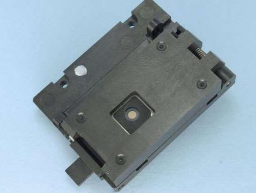
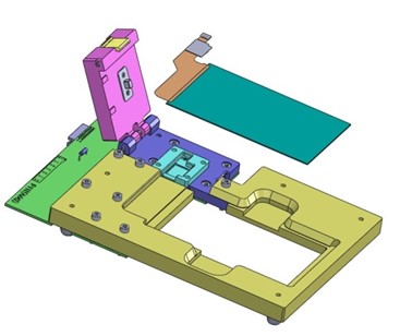
| Camera module |
 |
- Accurate alignment of the socket center to the camera module optical center.
Suitable for all kinds of module designs.
- Well experienced over 3,000 cases.
- Applicable of seamless implantation in-line production and off-line quality check.
|
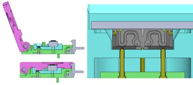
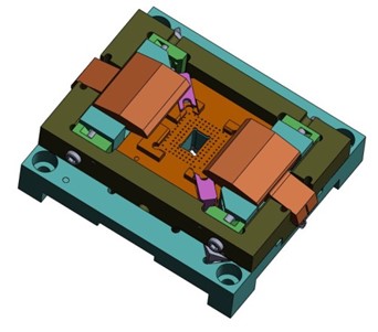
| Edge-contact module |
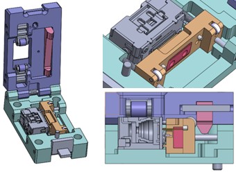 |
- Fitting to the specific test device, the PA is contacted from edge by pin module base while the optical center of the camera module device is still aligned from top.
|
| LCD display panel |
 |
- Applicable to all kinds of LCD display size and structure.
- Compact size and special custom design.
|
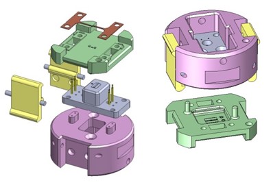
| Image sensor device |
 |
- Suitable for all kinds of image sensor package designs.
- Accurate alignment of the socket center to the optical center of the image sensor package.
- Applicable of seamless implantation in-line production and off-line quality check with flexible lead structures such as discrete, clamshell or cover-open types.
|
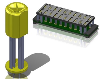
| LED, EELD, VCSEL chip on submounts |
 |
- Easy to loading and unloading CoS package devices.
- Special probe pin design to contact metal pads but without damage.
- Great thermal dissipation design and device temperature displaying.
|
| EELD TO package |
 |
- LD TO package (pitch: 1.43/2.0/2.54/5.08 mm)
- Special metal reed design to contact electrode pins without causing scratch damage.
- Lifetime: >10K cycles
- High current (> 5A) operation
- Available to array module for reliability aging test.
|
| Evaluation test board with sockets |
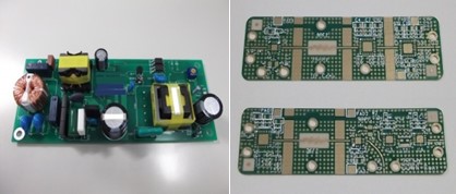 |
- High current/voltage design
- Low signal design (optoelectronic image sensor)
- High frequency /high speed design
- Compact and high integration design (multi-layers, BGA ,etc.)
|