Firmly stick to the WORTH
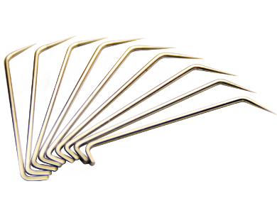
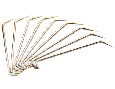
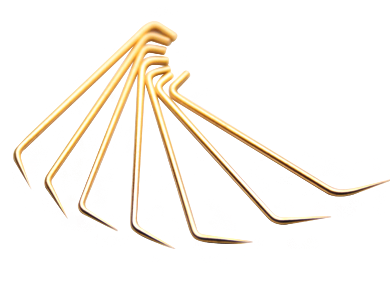
Both LED chip probing and map/sorting technology are significant during LED product manufacturing process. The contact probes are mainly utilized in chip probing for characterizing LED opto-electronic output characteristics such as output power, emission wavelength, voltage, ESD and etc., then to do sorting into variant bins for further assembly process. They are important in back end process for LED chip quality control and cost reduction.
In this case, G.C Micro provides reliable probes with our own manufacturing processes with IPs issued in Taiwan:
- patent no. M426768
- patent no. M429100
- patent no. M506970
And, G.C Micro has been certificated by ISO 9001 since 2014. We dedicate on stabilizing product quality and professional service to all customers, and are open mind to work with customers for custom specialized demands and provide trustworthy consuming materials for empowering our competitiveness.